- 您现在的位置:买卖IC网 > Sheet目录287 > 25LC160B-I/PG (Microchip Technology)IC EEPROM 16KBIT 10MHZ 8DIP
25XX160A/B
1.0
ELECTRICAL CHARACTERISTICS
Absolute Maximum Ratings (?)
V CC .............................................................................................................................................................................7.0V
All inputs and outputs w.r.t. V SS ......................................................................................................... -0.6V to V CC +1.0V
Storage temperature .................................................................................................................................-65°C to 150°C
Ambient temperature under bias ...............................................................................................................-40°C to 125°C
ESD protection on all pins ..........................................................................................................................................4 kV
? NOTICE : Stresses above those listed under “Absolute Maximum Ratings” may cause permanent damage to the
device. This is a stress rating only and functional operation of the device at those or any other conditions above those
indicated in the operational listings of this specification is not implied. Exposure to maximum rating conditions for an
extended period of time may affect device reliability.
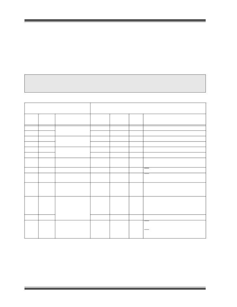
TABLE 1-1:
DC CHARACTERISTICS
DC CHARACTERISTICS
Industrial (I):
Automotive (E):
T AMB = -40°C to +85°C
T AMB = -40°C to +125°C
V CC = 1.8V to 5.5V
V CC = 2.5V to 5.5V
Param.
No.
D001
D002
D003
D004
D005
D006
D007
Sym.
V IH1
V IH2
V IL1
V IL2
V OL
V OL
V OH
Characteristic
High-level input
voltage
Low-level input
voltage
Low-level output
voltage
High-level output
Min.
2.0
0.7 V CC
-0.3
-0.3
—
—
V CC -0.5
Max.
V CC +1
V CC +1
0.8
0.2 V CC
0.4
0.2
—
Units
V
V
V
V
V
V
V
Test Conditions
V CC ≥ 2.7V (Note)
V CC < 2.7V (Note)
V CC ≥ 2.7V (Note)
V CC < 2.7V (Note)
I OL = 2.1 mA
I OL = 1.0 mA, V CC < 2.5V
I OH = -400 μ A
voltage
D008
D009
I LI
I LO
Input leakage current
Output leakage
—
—
±1
±1
μ A
μ A
CS = V CC , V IN = V SS TO V CC
CS = V CC , V OUT = V SS TO V CC
current
D010
C INT
Internal Capacitance
—
7
pF
T AMB = 25°C, CLK = 1.0 MHz,
(all inputs and
outputs)
V CC = 5.0V (Note)
D011
I CC Read
—
6
mA
V CC = 5.5V; F CLK = 10.0 MHz;
SO = Open
Operating Current
—
2.5
mA
V CC = 2.5V; F CLK = 5.0 MHz;
SO = Open
D012
D013
I CC Write
I CCS
—
—
3
5
mA
μ A
V CC = 5.5V
CS = V CC = 5.5V, Inputs tied to V CC or
Standby Current
V SS , T AMB = -40°C TO +125°C
—
1
μ A
CS = V CC = 2.5V, Inputs tied to V CC or
V SS , T AMB = -40°C TO +85°C
Note:
This parameter is periodically sampled and not 100% tested.
DS21807D-page 2
? 2007 Microchip Technology Inc.
发布紧急采购,3分钟左右您将得到回复。
相关PDF资料
25LC256T-E/MF
IC EEPROM 256KBIT 10MHZ 8DFN
25LC320A-I/P
IC EEPROM 32KBIT 10MHZ 8DIP
25LC512-E/MF
IC EEPROM 512KBIT 20MHZ 8DFN
25LC640-E/P
IC EEPROM 64KBIT 2MHZ 8DIP
25LC640A-E/P
IC EEPROM 64KBIT 10MHZ 8DIP
281708-4
PLUG HE14 IDC 90 4 P TUBE
281709-4
PLUG HE13 IDC 90 4 P AWG 24
281711-2
PLUG HE14 IDC 90 2 P TUBE
相关代理商/技术参数
25LC160B-I/PN
制造商:Microchip Technology Inc 功能描述:25LC160B-I/PN
25LC160B-I/S15K
功能描述:电可擦除可编程只读存储器 16K, 2K X 8, 32B PAGE, 2.5V SER EE, DIE in WAFFLE PK RoHS:否 制造商:Atmel 存储容量:2 Kbit 组织:256 B x 8 数据保留:100 yr 最大时钟频率:1000 KHz 最大工作电流:6 uA 工作电源电压:1.7 V to 5.5 V 最大工作温度:+ 85 C 安装风格:SMD/SMT 封装 / 箱体:SOIC-8
25LC160B-I/SN
功能描述:电可擦除可编程只读存储器 2kx8 32B - 2.5V RoHS:否 制造商:Atmel 存储容量:2 Kbit 组织:256 B x 8 数据保留:100 yr 最大时钟频率:1000 KHz 最大工作电流:6 uA 工作电源电压:1.7 V to 5.5 V 最大工作温度:+ 85 C 安装风格:SMD/SMT 封装 / 箱体:SOIC-8
25LC160B-I/SN
制造商:Microchip Technology Inc 功能描述:IC EEPROM 16K SMD 25LC160
25LC160B-I/SNG
功能描述:电可擦除可编程只读存储器 2kx8 32B - 2.5V Lead Free Package
RoHS:否 制造商:Atmel 存储容量:2 Kbit 组织:256 B x 8 数据保留:100 yr 最大时钟频率:1000 KHz 最大工作电流:6 uA 工作电源电压:1.7 V to 5.5 V 最大工作温度:+ 85 C 安装风格:SMD/SMT 封装 / 箱体:SOIC-8
25LC160B-I/ST
功能描述:电可擦除可编程只读存储器 2kx8 32B - 2.5V RoHS:否 制造商:Atmel 存储容量:2 Kbit 组织:256 B x 8 数据保留:100 yr 最大时钟频率:1000 KHz 最大工作电流:6 uA 工作电源电压:1.7 V to 5.5 V 最大工作温度:+ 85 C 安装风格:SMD/SMT 封装 / 箱体:SOIC-8
25LC160B-I/STG
功能描述:电可擦除可编程只读存储器 2kx8 32B - 2.5V Lead Free Package
RoHS:否 制造商:Atmel 存储容量:2 Kbit 组织:256 B x 8 数据保留:100 yr 最大时钟频率:1000 KHz 最大工作电流:6 uA 工作电源电压:1.7 V to 5.5 V 最大工作温度:+ 85 C 安装风格:SMD/SMT 封装 / 箱体:SOIC-8
25LC160B-I/W15K
功能描述:电可擦除可编程只读存储器 16K, 2K X 8, 32B PAGE, 2.5V SER EE, WAFER RoHS:否 制造商:Atmel 存储容量:2 Kbit 组织:256 B x 8 数据保留:100 yr 最大时钟频率:1000 KHz 最大工作电流:6 uA 工作电源电压:1.7 V to 5.5 V 最大工作温度:+ 85 C 安装风格:SMD/SMT 封装 / 箱体:SOIC-8
